Wi-Node - Build Guide
Building a Wi-Node - in Words and Pictures
Guide created and maintained by: Ian Chilton - please direct any suggestions or corrections to: ian [at] ichilton [dot] co [dot] uk.
If you get stuck, there is a Nanode Mailing List and an IRC channel - #nanode on irc.freenode.net.
Introduction
The Wi-Node can be used in two modes - either as a shield (or backpack) for an existing Arduino/Nanode or as a standalone node.
It's the standalone node we will be building here. We will build the basic node and then add optional additional functions and the components required for each. A separate Wi-Node Backpack Guide is available for users wishing to build as a shield to fit to an existing Nanode 5.
If you are not familar with the Nanode, see my blog post introducing the Nanode and my blog post introducing the Nanode RF & Wi-Node.
To sumarise, the Wi-Node is an Arduino compatible board with RFM12B wireless, SRAM, Micro-SD card and a motor driver.
I am maintaining a a page of useful Nanode links which are worth keeping an eye on as there is information like pin usage and pointers to useful code and libraries.
Some other useful information:
Building a Wi-Node is just a case of replicating the steps shown in the following picture sequence - no real electronics experience needed - just basic soldering skills.
The pcb is built in an orderly sequence starting with the resistors and small components that are low on the board and then working up to the bulkier parts like connectors. After soldering each component, you need to cut off the excess lead from the bottom using some cutters.
It is very easy to cause shorts which will make the board or specific parts of it not work. What i'd advise is that you take your time during the build, be precise, use minimal solder and carefully check each joint after soldering it. If you suspect any short, check it with a multimeter and fix any shorts there and then, before continuing.
Even if you have been soldering for years, i'd highly recommend these videos to get the right tools and improve your technique:
- EEVBlog Soldering Tutorial - Part 1: Tools
- EEVBlog Soldering Tutorial - Part 2: Soldering
- EEVBlog Soldering Tutorial - Part 3: Surface Mount
It's recommended you read through the whole of this guide and familiarise yourself with the steps before you start the actual build.
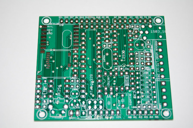
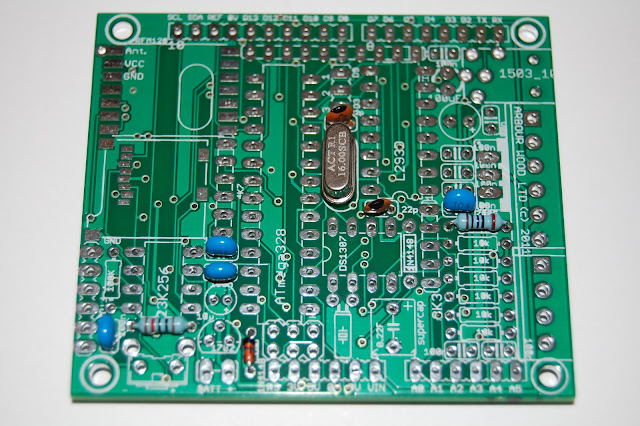
Step 1 - Identify Components and Kit Contents
Layout and identify the components from the kit.
The exact kit contents will vary depending on which kit you bought and any optional extras purchased.
Here are the components required to build the base node, plus wireless:
 |
| From Wi-Node Build |
 |
| From Wi-Node Build |
Pictured above is:
- The Wi-Node PCB
-
IC's (supplied on the black foam):
- ATMega328 - IC1: the main microcontroller
- 28-Pin DIL Socket - supplied in the black foam
- RFM12B Radio Module (optional)
- 16Mhz Crystal - Y1: for the ATMega328
- Switch - S1: for resetting the board
- MCP1702-3302 - IC2: 3.3v voltage regulator
- 1N4148 Diode - D1
- 3mm Green LED - LED1
- 4x 100nF Ceramic Capacitors - C1, C2, C3, C4
- 2x 22pF Ceramic Capacitors - C14, C15
- 10uF Electrolytic Capacitor - C5
- 6-way right-angle programming header
- 4x SIL Sockets - for arduono shield compatibility - SV1, SV2, SV4, SV4
- Antenna for the RFM12B (optional)
- 10k 1% Resistor (Brown, Black, Black, Red) - R1
- 100R Resistor (Brown, Black, Black, Black) - R10
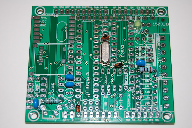
On top of those, additional components can be added to provide additional functions - as sketched out here:
 |
| From Wi-Node Build |
Note, there is an error in the above photo - the block of 4 resistors at the bottom right (R8, R9, R2 and R4) are labelled motor, but are actually for the analogue inputs. I'm also missing C12 and C13 labels at the bottom right. New version will follow.
The green highlighted components are those listed above and are needed to build an Arduino like bare Wi-Node board.
We can also see from this what components are required for each of the optional components:
- Analogue inputs - there are three options for these:
- For 3V3 analogue inputs (connecting straight to the ATMega328), Replace R8, R9, R2 and R4 (bottom right of the board behind the screw terminals, marked 10k) with wire links. Do not fit RN1 or C12 or C13.
- 10.25V Inputs (almost exaxtly 10mV increments per count) - R8, R9, R2 and R4 (bottom right of the board behind the screw terminals, marked 10k) are to be fitted with 10k resistors and RN1 (to the left of those resistors) to be fitted with a 4K7 resistor network.
- 36V Inputs (in roughly 35mV increments per count) - as per above, but fit a 1K resistor network to RN1.
- If you are using the latter two options, you can also fit 2x optional 100nF Ceramic Capacitors - C12, C13 to make a low pass filter on A0 and A1 with the 10K resistor which filters out any noise above about 1600Hz.
- It's worth noting that if you use the 10.25V or 36V options, you will not be able to use the analogue pins as digital input/output pins.
- 2x 2-way screw terminals - JP6 (optional)
-
23K256 SPI SRAM - provides extra SRAM for additional data storage. This is accessed using the SPI bus and digital pin 9 as a slave select. Please note that this can not be used at the same time as the L293D as they share the use of digital pin 9:
- 23K256 DIP SRAM IC - IC3
- 100k Resistor (Brown, Black, Black, Orange) - R11
- An optional 0.22F super capacitor so the contents of the RTC and SRAM are not lost when the power is removed (shared with the RTC) - C16
-
Real Time Clock - this provides a real time clock using the I2C bus (Analogue pins 4 & 5) with the interrupt/wake up alarm on digital pin 3:
- Either a Microchip MCP7941x (includes RTC, SRAM, EEPROM and Unique ID) SOIC or a Maxim/Dallas DS1307 DIP (IC5) or SOIC (U$4). There is an 8 pin DIP slot on the top of the board or an 8 pin SOIC slot on the bottom of the board - only one of these should be populated at a time.
- 2x 10k Resistors (Brown, Black, Black, Red) - R3 and R5.
- 1N4148 Diode - D2
- 32.768khz Crystal - Y2
- An optional 0.22F super capacitor so the contents of the RTC and SRAM are not lost when the power is removed (shared with the 23K256 SRAM) - C16
- 2x 22pF capacitors (it's only recently been found that these are required so these may not have been included in your kit)
-
L293D Motor Driver - Provides a quadruple high-current half-H driver - designed to provide bidirectional drive currents. This uses digital 4, 5, 6 (shared with the LED) and 7 as inputs. Digital pin 9 is used to enable outputs 1 & 2 (therefore this can not be used at the same time as the 23K256 SRAM) and outputs 3 & 4 are either enabled also by digital pin 9 (if JP4 is shorted between pins 1 & 2) or by digital pin 3 (if JP4 is shorted between pins 2 & 3, which stops the use of the interrupt/wake-up function of the MCP7941x). Using the LS293D also stops the use of the Micro SD card as they share the use of digital pin 4. Use of the L293D requies the addition of a 7805 5v voltage regulator and associated capacitors.
- L293D - quadruple high-current half-H driver IC - IC4
- 100uF Electrolytic Capacitor - C17
- 5x 100nF Ceramic Capacitors - C6, C7, C8, C9, C11
- 7805 5v Voltage Regulator - IC6
- 2x 3-way screw terminals - JP3 (optional)
-
Micro SD Card Slot - allows use of a micro sd card for storate. Uses the SPI bus and digital pin 4 as a slave select pin (Please note that this can not be used at the same time as the L293D as they share the use of digital pin 4):
- Micro SD Card Holder
-
Power & Serial Socket:
- A 4-pin jack socket - X1 is provided to supply GND, VIN, RX and TX. It's at the top right-hand side of the board and labelled on the board as 1503_10. This is not covered in the guide as it's not included in any of the kits and left as an optional extra for advanced users.
It's worth noting the operation of the 3 resistor networks:
- RN1 (at the right hand side of the board next to the RTC, labelled 3k3) is for the analogue pins, A0, A2, A2 and A3 and should be fitted if you wish to use these pins as high voltage inputs. For normal use it can be removed and R2, R4, R8 and R9 (at the right hand side of the board, labelled 10k) replaced with wire links.
- RN2 (at the left hand side of the board next to the micro SD slot, incorrectly labelled 4K7) is for level conversion when using the board as a shield for an existing Arduino/Nanode. When using the board as a standalone node, this should not be fitted. When using the board as a shield, a 10K resistor network should be fitted (see separate build guide.
- RN4 (at the top of the board, to the right of the RFM12B and above the ATMega328) is for level conversion when using the board as a shield for an existing Arduino/Nanode. When using the board as a standalone node, these should just be populated with wire links on pins 1->2, 3->4, 5->6, 7->8, 9->10.
Ok, we're ready to start. Here is the PCB ready:
 |
| From Wi-Node Build |
Step 2 - 10k Resistor
Start with the resistors. Bend each leg of the resistor over 90 degrees, right next to the body. The last colour on all of the resistors is brown - it's recommended that you align them all in the same direction and have the brown at the same end.
First we add the 10K resistor - it's colour code is Brown, Black, Black, Red. It's at the left hand side above the reset switch.
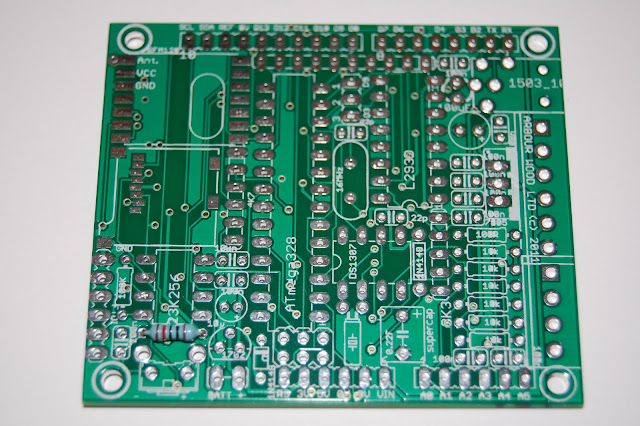 |
| From Wi-Node Build |
Step 3 - 100R Resistor
Add the 100R resistor - it's colour code is: Brown, Black, Black, Black. It's at the right hand side of the board at the top of the row of resistors.
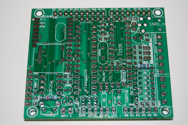 |
| From Wi-Node Build |
Step 4 - 1N4148 Diode
Add the 1N4148 diode - this protects the programming interface from any current from an external power supply. It's at the bottom of the board, to the right of the reset switch.

Step 5 - 100nF Ceramic Capacitors
Add the four 100nF ceramic capacitors, as per the photo. They are blue and marked 104. One on the left next to the programming header, two to the right of the 23K256 slot and one on the right above the 100R resistor.
 |
| From Wi-Node Build |
Step 6 - 22pF Ceramic Capacitors
Add the two 22pF ceramic capacitors. They have black marked tops, are marked 22 and go either side of the 16Mhz crystal (at the right of the ATMega328).
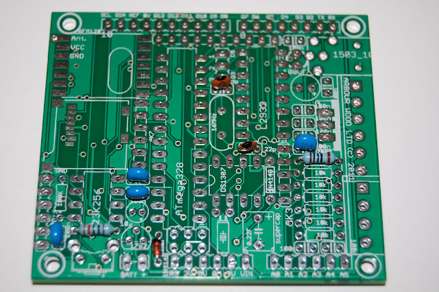 |
| From Wi-Node Build |
Step 7 - Crystal
Add the 16Mhz crystal - to the right of the ATMega328.
 |
| From Wi-Node Build |
Step 8 - LED
Add the green LED - it's at the top right hand side of the board, next to pin 8 of the L293D. The long leg should go to the top of the board and the shot leg and flat edge should go towards the bottom of the board.
 |
| From Wi-Node Build |
Step 9 - FTDI / Programming Adapter Header
The 6-way right angle header goes at the bottom left of the board. It's used to both program and power the board.
 |
| From Wi-Node Build |
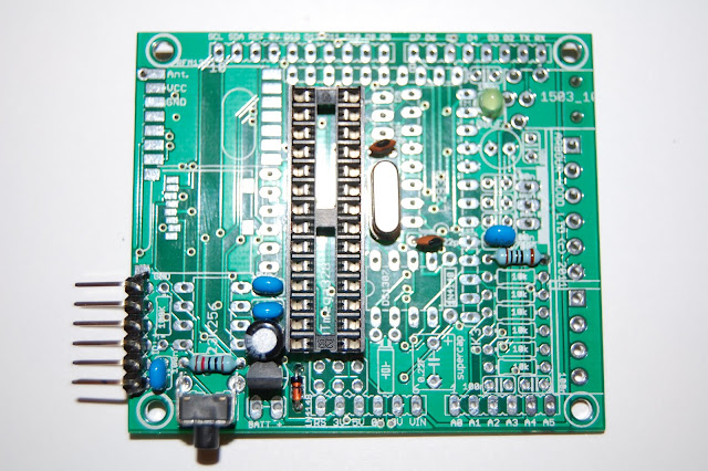
Step 10 - MCP1702 Voltage Regulator
Add the MCP1702 3.3v voltage regulator - it's at the bottom left next to the reset switch. The flat edge goes towards the bottom of the board. You should just need to bend the middle pin outwards slightly and insert it into the holes.
 |
| From Wi-Node Build |
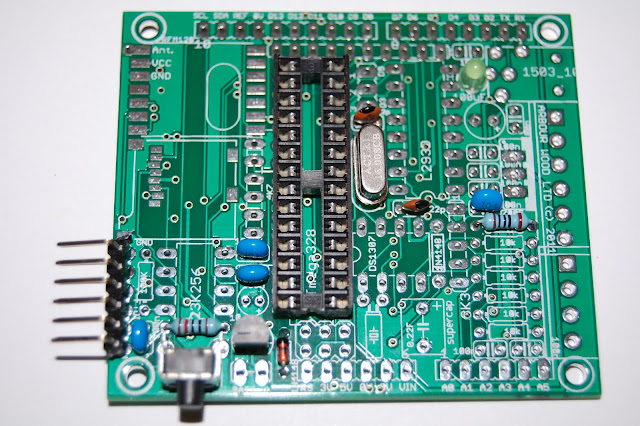
Step 12 - DIL Socket
Fit the DIL socket for the ATMega328. Note that one end has a small notch in it - this signifies pin 1 and should match up with the notch on the legend. It's best to tack diagonally opposite corners to hold the socket in place whilst the rest of the pins are soldered. Make sure they are fitted flat on to the board.
Note: If you are going to fit the optional RFM12B module, it's recommended you leave the DIL Socket until after Step 15 to give more space to get in and solder the RFM12B.
 |
| From Wi-Node Build |
Step 12 - Reset Switch
Add the reset switch at the bottom left of the board.
 |
| From Wi-Node Build |
Step 13 - 10uF Electrolytic Capacitors
Fit the 10uF Electrolytic capacitor just above the MCP1702 on the left hand side of the board. Ensure it is fitted the correct way round. The long leg needs to go to the + symbol on the legend and you will be able to see the white side on the photo (which goes towards the left of the board).
 |
| From Wi-Node Build |
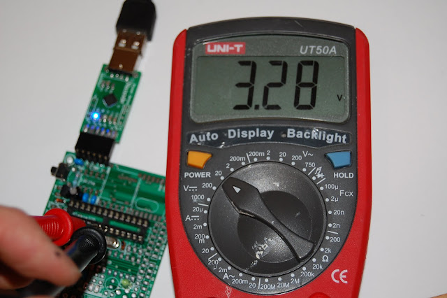
Step 14 - Voltage Check
You have nearly completed the board. However, before we add any of the (expensive) IC's, we need to check that they will receive the correct voltage.
Use a multimeter (in DC mode) to measure the voltage between pin 7 (GND) and pin 8 (VCC) of the ATMega328, as shown in the photo. You should receive something around 3.3v.
 |
| From Wi-Node Build |
It's also worth testing the pads marked VCC and GND on the RFM12B's spot - just to double check out of paranoia! - they should also read around 3.3v.
WARNING: Only proceed if all of your voltage readings from above are correct - if they weren't then you have a problem with your build.
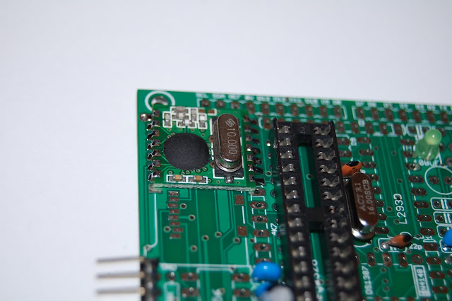
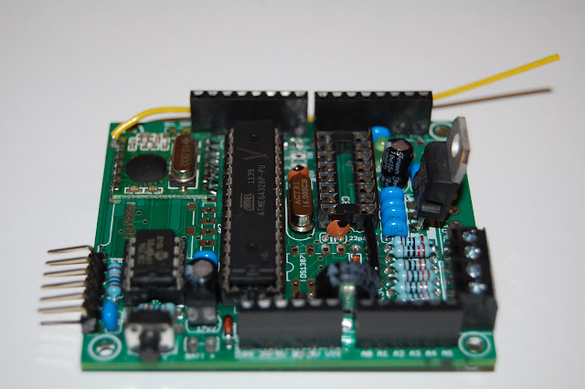
Step 15 - RFM12B - Optional
If you are going to fit the optional RFM12B wireless module. Place the module on the pads (observe the orientation - crystal to the inside) and solder each pad onto the board from above. It's worth doing opposite corners first to hold it in place, before doing the remaining pads.
 |
| From Wi-Node Build |
 |
| From Wi-Node Build |
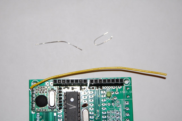
Step 16 - RFM12B Antenna - Optional
If you fitted the RFM12B module, you need to add an antenna - this is a piece of wire of approx 82mm, which will act as a quarter wave for the 868Mhz RF.
 |
| From Wi-Node Build |
If you didn't fit the DIL socket earlier, as advised - you can fit that now.
Step 17 - Arduino Shield Connectors - Optional
Add the Arduino shield connectors. There are 2 x 6 way and 2 x 8 way SIL sockets. Make sure you get them in the inner lines of holes and that they are fitted straight and vertical. Best to tack one end pin whilst you hold them straight - check the alignment then solder the remaining pins in place. You could also use a shield to keep them aligned if you have one handy.
 |
| From Wi-Node Build |
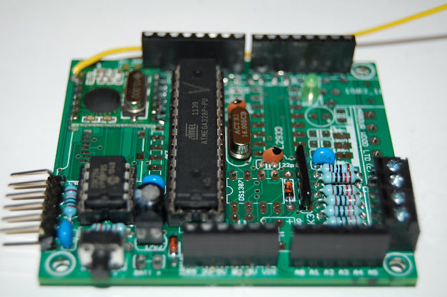
Step 18 - ATMega328 IC
Add the ATMega328 IC into the socket. Note the spot next to pin 1 and ensure you insert it in the right way.
IC's usually come with their legs pointing slightly outwards. To get them to fit easily into the socket, you should put the legs flat on a desk and rock the IC slightly to bend the pins inwards - do that at both sides and try again to fit into the socket.
 |
| From Wi-Node Build |
 |
| From Wi-Node Build |
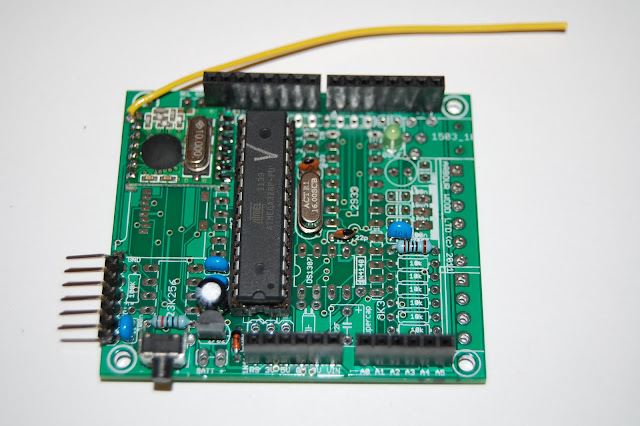
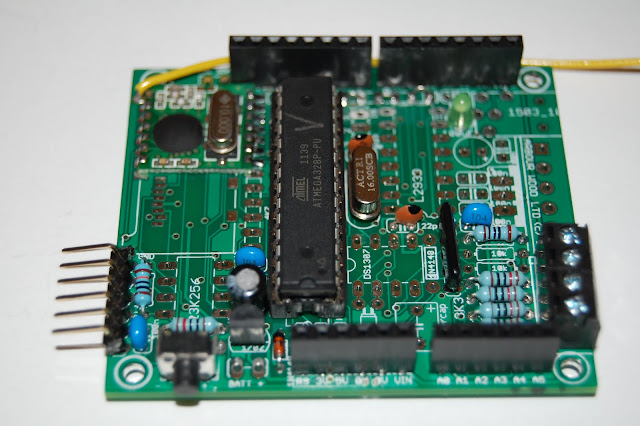
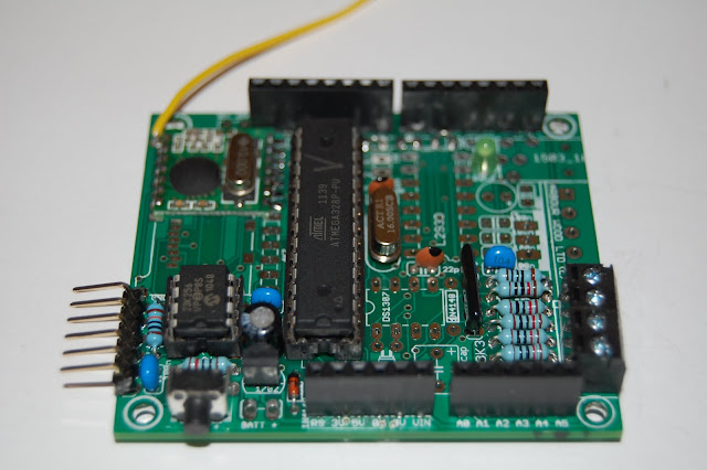
This concludes the build of the base board.
 |
| From Wi-Node Build |
We'll now look at the different optional steps you may wish to consider.
Step 20 - Wire Links (Optional)
In order to use digital pins 4, 9, 10, 11 and 13 from the shield connectors, we need to fit some wire links instead of RN4 (which is required when using the Wi-Node as a backpack.
Fit 5 separate wire links between the following pins: 1 and 2, 3 and 4, 5 and 6, 7 and 8, 9 and 10.
I used some of the component leg cut-off's and bent it over a pair of plyers.

Step 21 - Analogue Inputs (Optional)
Refer to the information in Step 1 about the options available for the Analogue inputs.
Step 21a: Option 1 - 3V3 Analogue Inputs:
For 3V3 analogue inputs (connecting straight to the ATMega328), Replace R8, R9, R2 and R4 (bottom right of the board behind the screw terminals, marked 10k) with wire links. Do not fit RN1 or C12 or C13.

Step 21a: Option 2 - 10.25v Analogue Inputs:
10.25V Inputs (almost exaxtly 10mV increments per count) - R8, R9, R2 and R4 (bottom right of the board behind the screw terminals, marked 10k) are to be fitted with 10k resistors and RN1 (to the left of those resistors) to be fitted with a 4K7 resistor network.

Step 21a: Option 3 - 16v Analogue Inputs:
36V Inputs (in roughly 35mV increments per count) - R8, R9, R2 and R4 (bottom right of the board behind the screw terminals, marked 10k) are to be fitted with 10k resistors and RN1 (to the left of those resistors) to be fitted with a 1K resistor network.
Step 21b - Low Pass Filter on A0 and A1 (Optional):
If you are using the options 2 or 3 above, you can also fit 2x optional 100nF Ceramic Capacitors - C12, C13 to make a low pass filter on A0 and A1 with the 10K resistor which filters out any noise above about 1600Hz.

Step 21c - Screw Terminals (Optional):
Screw terminals can be added for ease of access to the analogue inputs: A0, A1, A2 and A3.

Step 22 - 23K256 SRAM (Optional)
Refer to the information in Step 1 for more information about the 23K256 SRAM.
Step 22a - 100k Resistor
Fit the 100k Resistor (Brown, Black, Black, Orange) at the bottom left of the board, behind the programming header.
Step 22b - 8-Pin DIL Socket
Fit the 8-pin DIL socket in the bottom left corner of the board, above the reset switch. Note that the notce (pin 1) should be facing towards the bottom of the board.


Step 22c - Fit 23K256 IC
Fit the 23K256 IC, ensuring that the notch lines up with the notce on the socket.

Step 22d - 0.22F Super Capacitor (Optional)
If you wish to keep the memory contents of the 23K256 and RTC when the power is removed, fit a 0.22F super capacitor. This goes in the bottom middle of the board, under the DS1307 DIL socket (to the right of the ATMega328). It is supplied unpolarised and can be fitted either way. I usually put the flat side to negative and have the arrows pointing to positive.
I'm going to fit this after the RTC components - see step 23e for photo if you are not doing the RTC and want to fit the super capacitor now.
Step 23 - Real Time Clock (Optional)
Refer to the information in Step 1 for more about the RTC.
There are two options here - a DIP socket on the top of the board or SOIC pads on the bottom of the board. Both Dallas DS1307 and Microchip MCP7941x IC's are supported. I'll cover adding an MPC7941x in the SOIC slot here as that's what's included in the Wi-Node kits if your choose kit includes the RTC option. Either a MCP79410 or an MPC79411 may be used - the only difference is the latter has it's unique id area pre-programmed with a unique ethernet MAC address.
Step 23a - MCP7941x IC
First locate the SOIC pads - they are on the bottom of the board, to the right of the ATMega328. They are labelled DS1307SO8.

You should apply a small amount of solder to each pad (on the back of the board). Place the IC over the pads using some tweezers (ensure you note pin 1 to get it the corredct way). Use your soldering iron to heat one of the pins and melt the solder, affixing the IC to the board. If you tack opposite corners first, ensure it's placed correctly and then you can leisurely solder the remaining pins without fear of it moving.

Step 23b - 10k Resistors
Add the 2x 10k resistors (Brown, Black, Black, Red), R3 and R5. They are located at the right hand side of the board, are labelled 10k and are the two directly under the 100R fitted in step 3. There should be 4x 10k labelled spaces left below them.
Step 23c - 1N4148 Diode
Add the 1N4148 Diode, D2. This is to the right of the space for the DIP version. Ensure it goes the correct way round as per the markings. The black bar on the diode should be facing to the bottom of the board.
Step 23d - 32.768k Crystal
Add the very small, cylindrical 32.768k RTC crystal. This is under the space for the DIP version and can go either way round.

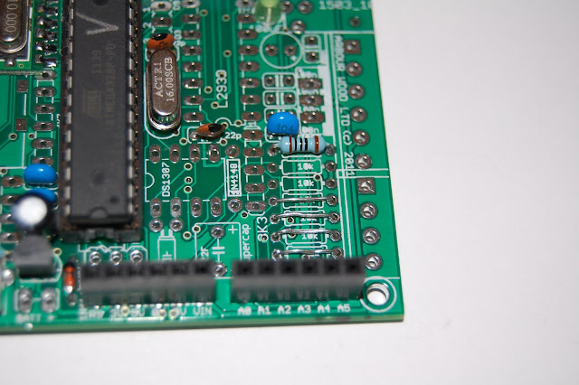
Step 23e - 0.22F Super Capacitor (Optional)
If you wish to keep the memory contents of the 23K256 and RTC when the power is removed, fit a 0.22F super capacitor. This goes in the bottom middle of the board, under the DS1307 DIL socket (to the right of the ATMega328). It is supplied unpolarised and can be fitted either way. I usually put the flat side to negative and have the arrows pointing to positive.

Step 23f - 22pF Ceramic Capacitors (MCP7941x only)
It has recently been found that if you use an MCP7941x chip you need to fit 2x 22pF capacitors, otherwise the clock loses around a minute a day. Fitting a 22pF between each leg of the 32.768khz crystal and ground fixes this problem. This is not required if you use a DS1307. Fortunately, the Wi-Node PCB contains space for either a DIL or an SOIC RTC chip, so you can do the other one to access the required pins. You should fit a 22pf capacitor between Pin 1 and Pin 4 (GND) and another between Pin 2 and Pin 4 (GND).
Step 24 - L293D Motor Driver (Optional)
Refer to the information in Step 1 for more about the L293D.
Step 24a - DIL Socket
Fit the 16-pin DIL socket. It goes to the right of the 16Mhz crystal with the notch (indicating pin 1) downwards.

Step 24b - 100nF Ceramic Capacitors
Fit the 5x 100nF ceramic capacitors, C6, C7, C8, C9 and C11.

Step 24c - 100uF Electrolytic Capacitor
Fit the 100uF Electrolytic, C17.

Step 24d - 7805 5v Voltage Regulator
Fit the 7805 Voltage Regulator.
Step 24e - Pin selection to enable outputs 3&4
The enable pin for outputs 3&4 can be changed between digital 9 so it will be enabled at the same time as outputs 1&2 and digital 3 where outputs 3&4 can be controlled separately at the expensve of the interrupt / wake up alarm from the RTC.

Step 24f - Screw Terminals (optional)
2x 3-way screw terminals can be fitted to provide easy access to GND, VIN and the four LS293D outputs.


Step 24g - L293D IC
Fit the L293D IC into the socket.

Step 25 - Micro SD Slot
To Follow.
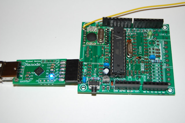
Step 26 - Test Board
Congratulations, you have completed the build of your Wi-Node
We can now see if you have done it successfully!
Connect a 5v FTDI cable or Nanode Programming Adapter to power the board. If after a few seconds you see the LED come on and start flashing then the microcontroller is working and running code. If not, you should remove power and check over the board and connections.
If you are using a Nanode programming adapter and your system prompts you for drivers, you can download those here.
If you are not using a Nanode programming adapter, you can use a normal FTDI lead but ensure the pinouts are as follows (left to right - left nearest the usb connector):
- 1 - GND
- 2 - Not Connected
- 3 - 5V
- 4 - TXD
- 5 - RXD
- 6 - RST (for auto reset)
If you have two boards with RFM12B modules, you can test them by using my RFM12B Test code.
If you have fitted the optional MCP7941x Real Time Clock, you can test that out by using my Arduino MCP7941x Library and running the example sketches.
I'm also aiming to provide code to test other aspects of the board and some working examples of Nanode/Wi-Node usage, but in the meantime i'm collecting useful code snippets and links on my Nanode Information Page.